- 您现在的位置:买卖IC网 > Sheet目录3872 > PIC18F4450T-I/ML (Microchip Technology)IC PIC MCU FLASH 8KX16 44QFN
136
XMEGA A [MANUAL]
8077I–AVR–11/2012
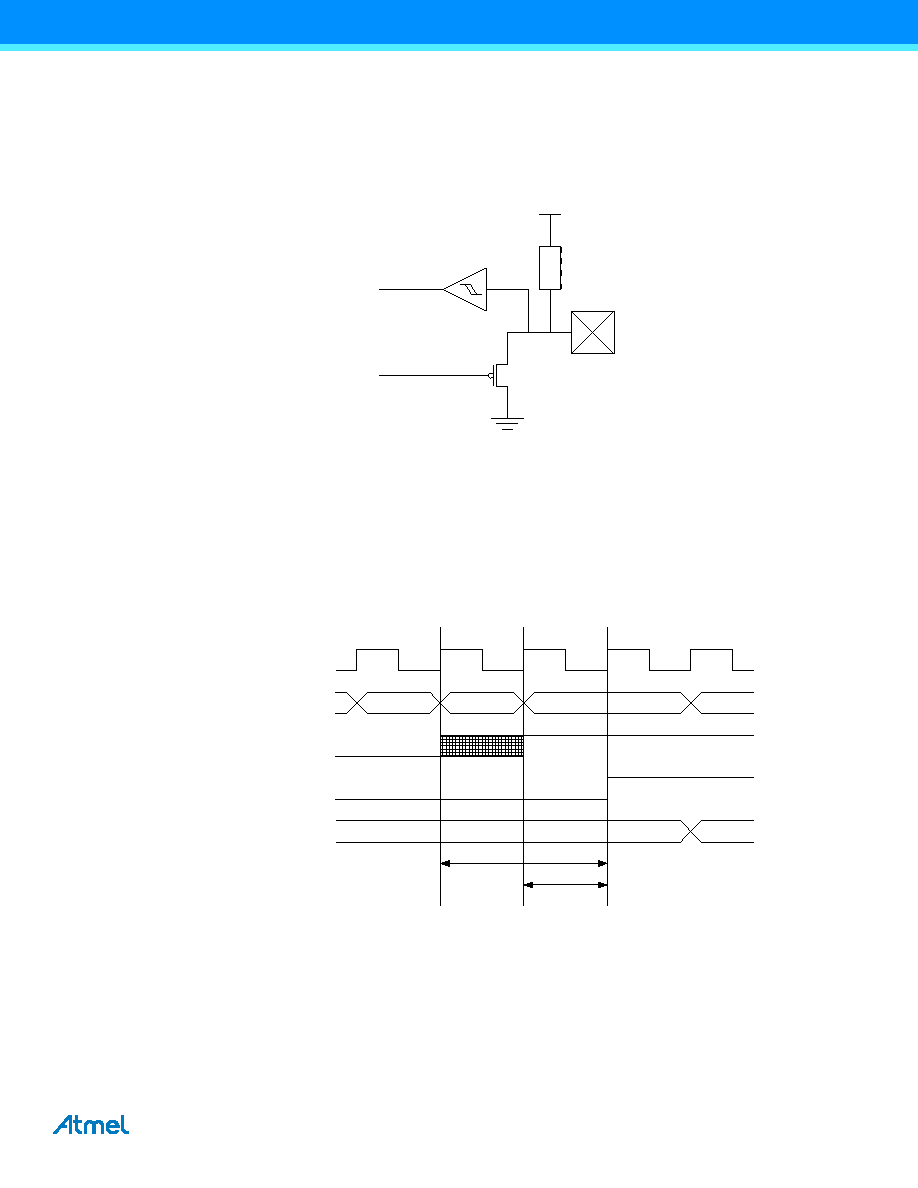
13.3.4 Wired-AND
In the wired-AND configuration, the pin will be driven low when the corresponding bits in the OUT and DIR registers are
written to zero. When the OUT register is set to one, the pin is released allowing the pin to be pulled high with the internal
or an external pull-resistor. If internal pull-up is used, this is also active if the pin is set as input.
Figure 13-7. Output configuration - Wired-AND with optional pull-up.
13.4
Reading the Pin Value
Independent of the pin data direction, the pin value can be read from the IN register, as shown in Figure 13-1 on page
133. If the digital input is disabled, the pin value cannot be read. The IN register bit and the preceding flip-flop constitute
a synchronizer. The synchronizer introduces a delay on the internal signal line. Figure 13-8 on page 136 shows a timing
diagram of the synchronization when reading an externally applied pin value. The maximum and minimum propagation
delays are denoted as tpd,max and tpd,min, respectively.
Figure 13-8. Synchronization when reading a pin value.
13.5
Input Sense Configuration
Input sensing is used to detect an edge or level on the I/O pin input. The different sense configurations that are available
for each pin are detection of a rising edge, falling edge, or any edge or detection of a low level. High level can be
detected by using the inverted input configuration. Input sensing can be used to trigger interrupt requests (IREQ) or
events when there is a change on the pin.
INn
OUTn
Pn
PERIPHERAL CLK
INSTRUCTIONS
SYNCHRONIZER FLIPFLOP
IN
r17
xxx
lds r17, PORTx+IN
tpd, max
tpd, min
0x00
0xFF
发布紧急采购,3分钟左右您将得到回复。
相关PDF资料
PIC18F4321T-I/ML
IC PIC MCU FLASH 4KX16 44QFN
PIC18F4221T-I/ML
IC PIC MCU FLASH 2KX16 44QFN
PIC18F2321T-I/ML
IC PIC MCU FLASH 4KX16 28QFN
PIC18F2221T-I/SO
IC PIC MCU FLASH 2KX16 28SOIC
PIC16LF1939-I/MV
IC MCU 8BIT 28KB FLASH 40-UQFN
PIC24F16KL402-I/SP
IC MCU 16BIT 16KB FLASH 28-SPDIP
PIC18F24J11-I/SS
IC PIC MCU FLASH 16K 2V 28-SSOP
PIC24F16KA101-I/SO
IC PIC MCU FLASH 16K 20-SOIC
相关代理商/技术参数
PIC18F4450T-I/PT
功能描述:8位微控制器 -MCU 16KB FL 768 RAM 34 I/O FS-USB 2.0 RoHS:否 制造商:Silicon Labs 核心:8051 处理器系列:C8051F39x 数据总线宽度:8 bit 最大时钟频率:50 MHz 程序存储器大小:16 KB 数据 RAM 大小:1 KB 片上 ADC:Yes 工作电源电压:1.8 V to 3.6 V 工作温度范围:- 40 C to + 105 C 封装 / 箱体:QFN-20 安装风格:SMD/SMT
PIC18F4455-BL
制造商:POWERLITE SYSTEMS 功能描述:PIC18F445 W/ BOOTLOADER FOR FLASHLAB 制造商:POWERLITE SYSTEMS 功能描述:PIC18F445 W/ BOOTLOADER, FOR FLASHLAB 制造商:POWERLITE SYSTEMS 功能描述:PIC18F445 W/ BOOTLOADER, FOR FLASHLAB; Silicon Manufacturer:Powerlite Systems; Core Architecture:PIC; Kit Contents:Board; Features:Bootloader Programming, RS232 Connector for Boot-Loading and Serial Comms ;RoHS Compliant: Yes
PIC18F4455-I/ML
功能描述:8位微控制器 -MCU 24kBF 2048RM FSUSB2 RoHS:否 制造商:Silicon Labs 核心:8051 处理器系列:C8051F39x 数据总线宽度:8 bit 最大时钟频率:50 MHz 程序存储器大小:16 KB 数据 RAM 大小:1 KB 片上 ADC:Yes 工作电源电压:1.8 V to 3.6 V 工作温度范围:- 40 C to + 105 C 封装 / 箱体:QFN-20 安装风格:SMD/SMT
PIC18F4455-I/P
功能描述:8位微控制器 -MCU 24kBF 2048RM FSUSB2 RoHS:否 制造商:Silicon Labs 核心:8051 处理器系列:C8051F39x 数据总线宽度:8 bit 最大时钟频率:50 MHz 程序存储器大小:16 KB 数据 RAM 大小:1 KB 片上 ADC:Yes 工作电源电压:1.8 V to 3.6 V 工作温度范围:- 40 C to + 105 C 封装 / 箱体:QFN-20 安装风格:SMD/SMT
PIC18F4455-I/PT
功能描述:8位微控制器 -MCU 24kBF 2048RM FSUSB2 RoHS:否 制造商:Silicon Labs 核心:8051 处理器系列:C8051F39x 数据总线宽度:8 bit 最大时钟频率:50 MHz 程序存储器大小:16 KB 数据 RAM 大小:1 KB 片上 ADC:Yes 工作电源电压:1.8 V to 3.6 V 工作温度范围:- 40 C to + 105 C 封装 / 箱体:QFN-20 安装风格:SMD/SMT
PIC18F4455T-I/ML
功能描述:8位微控制器 -MCU 24kBF 2048RM FSUSB2 RoHS:否 制造商:Silicon Labs 核心:8051 处理器系列:C8051F39x 数据总线宽度:8 bit 最大时钟频率:50 MHz 程序存储器大小:16 KB 数据 RAM 大小:1 KB 片上 ADC:Yes 工作电源电压:1.8 V to 3.6 V 工作温度范围:- 40 C to + 105 C 封装 / 箱体:QFN-20 安装风格:SMD/SMT
PIC18F4455T-I/PT
功能描述:8位微控制器 -MCU 24kBF 2048RM FSUSB2 RoHS:否 制造商:Silicon Labs 核心:8051 处理器系列:C8051F39x 数据总线宽度:8 bit 最大时钟频率:50 MHz 程序存储器大小:16 KB 数据 RAM 大小:1 KB 片上 ADC:Yes 工作电源电压:1.8 V to 3.6 V 工作温度范围:- 40 C to + 105 C 封装 / 箱体:QFN-20 安装风格:SMD/SMT
PIC18F4458-I/ML
功能描述:8位微控制器 -MCU 24KB Flash 2KB RAM RoHS:否 制造商:Silicon Labs 核心:8051 处理器系列:C8051F39x 数据总线宽度:8 bit 最大时钟频率:50 MHz 程序存储器大小:16 KB 数据 RAM 大小:1 KB 片上 ADC:Yes 工作电源电压:1.8 V to 3.6 V 工作温度范围:- 40 C to + 105 C 封装 / 箱体:QFN-20 安装风格:SMD/SMT